8086 Memory Interfacing: 2 RAM and 2 EEPROM Chips :- Interfacing RAM (Random Access Memory) and EEPROM (Electrically Erasable Programmable Read-Only Memory) chips with the 8086 microprocessor involves addressing and decoding mechanisms. The 8086 microprocessor has a 20-bit address bus, which allows it to address up to 220220 = 1 MB of memory.
Let’s consider the case where 2 RAM chips (16 K × 8) and 2 EEPROM chips (16 K × 8) are to be interfaced. Each chip has a capacity of 16 K bytes, and each byte is 8 bits.
Addressing for 8086:
The 8086 microprocessor has a 20-bit address bus, allowing it to address a total of 220=1 MB220=1 MB of memory locations.
- RAM Chips (16 K × 8):
- Each RAM chip requires 14 address lines (2^14 = 16 K).
- The 8086’s 20-bit address bus allows addressing up to 220=1 MB220=1 MB.
- Therefore, each RAM chip occupies a 16 K block within the address space.
- The two RAM chips would be connected to different address ranges within the total address space.
- EEPROM Chips (16 K × 8):
- Similar to RAM, each EEPROM chip requires 14 address lines.
- The two EEPROM chips would also be connected to different address ranges within the 1 MB address space.
Interfacing Circuit:
- Address Bus Connection:
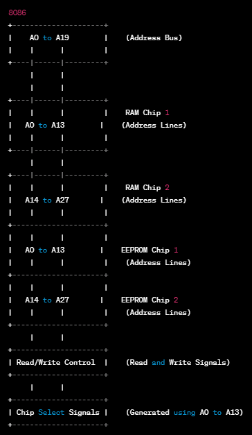
- Connect the 20-bit address bus of 8086 to the address inputs of all memory chips.
- For RAM chip 1, use A0 to A13 (14 address lines) and for RAM chip 2, use A14 to A27.
- For EEPROM chip 1, use A0 to A13, and for EEPROM chip 2, use A14 to A27.
- Chip Select Signals:
- Use the lower-order address lines (A0 to A13) to generate chip select signals for each chip.
- For RAM chip 1, the chip select signal would be active when A14 and above are high.
- For RAM chip 2, the chip select signal would be active when A0 to A13 are low and A14 and above are high.
- Similarly, generate chip select signals for EEPROM chips.
- Read/Write Control:
- Connect the Read and Write control signals from the 8086 to the corresponding control inputs of RAM and EEPROM chips.
In simpler terms, think of these connections like roads. The address wires are like the lanes that tell the chips where to go. The chip select signals are like traffic signals, guiding each chip when it’s their turn to pay attention. And the read/write control signals are like signs telling the chips whether to read information from the 8086 or write information to it. This way, everyone knows their role and can communicate effectively!
Here’s a simplified representation of the interfacing circuit:

Full Decoding Concept:
- The full decoding concept ensures that each memory chip responds only to its assigned address range. This is achieved by using appropriate combinations of address lines for chip selection.
- When the 8086 generates an address, the decoding logic enables the chip select signal for the specific memory chip that corresponds to the address range.
- For example, if the address falls within the range of RAM chip 1, the chip select signal for RAM chip 1 becomes active, allowing it to respond to read or write operations.
- This decoding mechanism ensures that each memory chip is accessed only when its specific address range is targeted, preventing conflicts and enabling a proper memory organization.
By following this addressing and decoding scheme, the interfacing circuit ensures efficient communication between the 8086 microprocessor and the two RAM chips and two EEPROM chips.
The full decoding concept is like making sure each memory chip knows when it’s its turn to work. Imagine you have different people in a room, and each one has a specific job to do. To make things run smoothly, we need a way for each person to know when it’s their turn to act.
Similarly, in our computer setup with the 8086 microprocessor, we have two RAM chips and two EEPROM chips. The full decoding concept helps us organize this so that each chip does its job at the right time.
When the 8086 microprocessor wants to talk to one of these chips, it sends out an address, like telling someone where to find you in a big room. The decoding logic is like a smart system that listens to this address and decides which chip needs to pay attention.
For example, let’s say the microprocessor sends out an address, and it’s in the range assigned to RAM chip 1. The decoding logic says, ‘Hey, RAM chip 1, this message is for you!’ It turns on a signal called chip select for RAM chip 1. This signal is like a spotlight that says, ‘Now it’s your turn to do some work.’
This way, each memory chip only responds when it hears its name (or address). RAM chip 1 doesn’t bother when the message is for EEPROM chip 2, and vice versa. This smart decoding mechanism ensures that each chip does its job only when it’s supposed to, avoiding confusion and making everything work smoothly.
So, in simple terms, this addressing and decoding system is like having a well-organized conversation where each person knows when to speak, preventing chaos and making sure the 8086 microprocessor can talk to the RAM and EEPROM chips without any confusion.