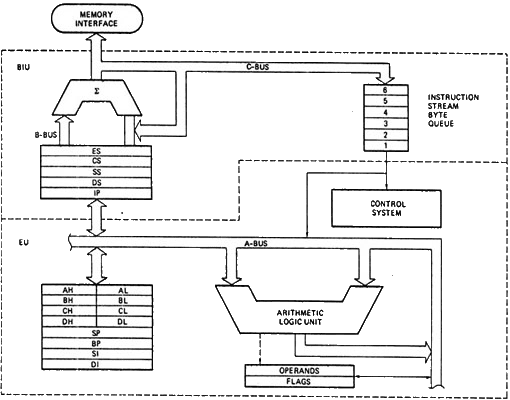
Block diagram of EU and BIU of 8086 Microprocessor

Discuss the working of EU and BIU of 8086 Microprocessor

Working of EU and BIU of 8086 Microprocessor: The 8086 microprocessor is comprised of two key execution units: the Execution Unit (EU) and the Bus Interface Unit (BIU). Each plays a distinct role in the overall operation of the processor. These units work together to execute instructions and manage data transfer between the microprocessor and memory or peripherals.
Execution Unit (EU):

  1. Function:
  • The EU is responsible for executing instructions. It performs arithmetic and logic operations on data as directed by the instructions in the program.
  • It includes the Arithmetic and Logic Unit (ALU) that performs mathematical and logical operations, as well as general registers to store data during computation.
  1. Registers:
  • The EU contains various registers, including general-purpose registers like AX, BX, CX, and DX, which are used for data manipulation.
  • The instruction pointer (IP) register keeps track of the address of the next instruction to be executed.
  1. Instruction Execution:
  • The EU fetches instructions from memory using the BIU.
  • Once an instruction is fetched, the EU decodes it to determine the operation to be performed and fetches any required operands.
  • The ALU then executes the operation, and the result is stored in the appropriate registers.

Bus Interface Unit (BIU):

  1. Function:
  • The BIU is responsible for managing the flow of data between the microprocessor and external devices, such as memory and I/O devices.
  • It provides the necessary control signals for the data bus and address bus.
  1. Segmentation:
  • The 8086 uses a divided memory style. The BIU manages the division of memory addresses, putting together a 16-bit part of the address from a register with a 16-bit shift to create a 20-bit actual address.
  1. Address Generation:
  • The BIU generates the physical memory address for fetching instructions and data. It combines the information of the segment registers (CS, DS, SS, ES) with the offset values to create the complete memory address.
  1. Bus Control:
  • The BIU manages the control signals for the system buses, including the address bus, data bus, and control bus.
  • It generates signals to control the flow of data between the microprocessor and memory or peripherals.

Interaction Between EU and BIU:

  1. Instruction Fetch:
  • The BIU fetches instructions from memory and places them in the instruction queue.
  • The EU then takes instructions from the queue, decodes them, and executes the corresponding operations.
  1. Data Transfer:
  • When data needs to be transferred between the microprocessor and memory or peripherals, the BIU handles the address generation and control signals.
  • The EU, on the other hand, manages the actual execution of instructions that involve data manipulation (Handling or controlling).
  1. Execution Flow:
  • The BIU and EU cooperate, with the BIU managing the external data and address pathways while the EU carries out the real execution of instructions.
  • The BIU ensures a smooth flow of data and instructions between the microprocessor and the external environment.

In summary, the Execution Unit (EU) of the 8086 is responsible for executing instructions, performing arithmetic and logic operations, and managing registers. The Bus Interface Unit (BIU) is responsible for managing data transfer between the microprocessor and external devices, handling address generation, and controlling the system buses. Together, these units allow the 8086 to fetch, decode, and execute instructions in a coordinated manner.

8086

How 8086 CLK and RESET signals are generated using 8284 ? Explain in detail?

Generating CLK and RESET Signals for 8086 using 8284, The clock and reset signals required for the operation of the 8086 microprocessor. The 8086 microprocessor itself doesn’t include an on-chip clock generator or reset circuitry, so external components are needed to provide these essential signals. The 8284 clock generator chip plays a crucial role in providing the 8086 microprocessor with its timing signals, the clock (CLK) and reset (RESET).

Generating CLK Signals for 8086 using 8284

The 8284 generates the clock signal (CLK) for the 8086 microprocessor. The clock is essential for synchronizing the operation of the microprocessor and other connected devices.

Crystal Oscillator:

The heart of the 8284 is a crystal oscillator. This component vibrates at a precise frequency determined by the attached quartz crystal. The crystal’s inherent properties ensure high accuracy and stability, making it ideal for generating the CPU’s timing reference.

Frequency Divider:

The output of the crystal oscillator is a high-frequency signal unsuitable for the 8086 directly. The 8284 has built-in dividers to reduce this frequency to the desired clock speed for the microprocessor. Typically, the input frequency is divided by three, resulting in a final clock frequency for the 8086.

Clock Generation:

The divided signal from the oscillator drives a clock circuit within the 8284. This circuit generates a square wave signal with a 50% duty cycle and the desired clock frequency. This signal becomes the CLK output of the 8284 and feeds the 8086, synchronizing its internal operations.

Connection to the 8086

8086
8086

The CLK signal generated by the 8284 is connected to the CLK pin of the 8086 microprocessor.

Generating RESET Signals for 8086 using 8284

The 8284 generates the RESET signal for the 8086 microprocessor. The RESET signal is used to initialize the microprocessor and set it to a known state. The 8284. This chip keeps an eye on the power supply and knows when the computer is turned on or off. Whenever the computer is turned on or restarted, the 8284 chip sends a special signal (reset pulse) to the microprocessor, telling it to clear its memory and get ready to start working again.

  • The 8284 includes a reset generator circuit that monitors the power supply and generates a reset pulse when power is applied or restored.
  • The RESET signal is also generated when the microprocessor is initially powered on or when the system is reset.
  • Additionally, the 8284 provides a Manual Reset input (MR), which allows external control of the reset function. When Manual Reset is pulled low, a reset pulse is generated, forcing the 8086 into a known state.

Connection to the 8086

8086
8086

The RESET signal generated by the 8284 is connected to the RESET pin of the 8086.

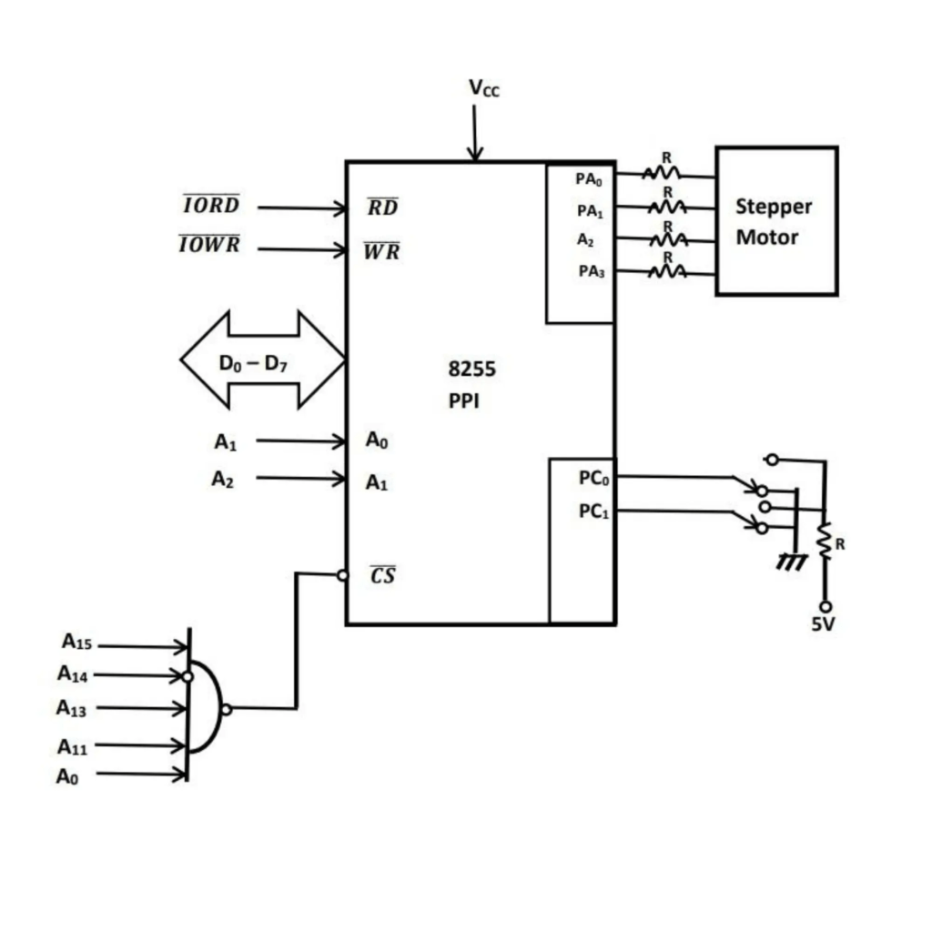
Interfacing Stepper Motor to 8086 using 8255 Diagram

Explain with a neat diagram the interfacing of stepper motor to 8086 using 8255 in detail

The integration of a stepper motor with an 8086 microprocessor is made seamless through the use of the 8255 Programmable Peripheral Interface (PPI). The detailed walkthrough, complete Interfacing of Stepper Motor to 8086 using 8255 with a connection diagram and programming insights, to empower enthusiasts and engineers in the realm of microprocessor-controlled stepper motor applications.

Components Overview:

  1. 8086 Microprocessor:
    • The central processing unit that governs the overall system.
  2. 8255 PPI:
    • A programmable chip that extends additional Input/Output (I/O) ports to the 8086, facilitating communication with external devices.
  3. Stepper Motor:
    • A specialized motor that rotates in precise increments, responding to electrical pulses.
  4. Driver Circuit:
    • An electronic circuit responsible for amplifying signals from the 8255, which are then used to drive the coils of the stepper motor.

Connection Diagram:

  • Data Lines:
  • Connect the data lines (D0-D7) of the 8255 to the corresponding data lines of the 8086 for data transfer.
  • Address/Control Lines:
  • Link the address/control lines (A0-A2, CS, RD, WR) of the 8255 to the corresponding lines on the 8086 used for I/O operations.
  • Ports:
  • Port A/B:
    • Connect the four bits of Port A or B (PA0-PA3 or PB0-PB3) to the driver circuit, controlling the stepper motor coils.
  • Port C:
    • Use Port C (PC0-PC7) for additional control signals such as direction, step pulse, and enable.

Programming:

  • Employ Assembly Language Programming (ALP) to configure 8255 ports and govern the stepper motor.
  • Set the appropriate mode for Ports A/B and Port C using the control registers of the 8255.
  • Write the desired bit sequence to Ports A/B to energize the stepper motor coils for rotation.
  • Use Port C for controlling direction, step pulse timing, and enabling/disabling the motor.

Operation:

  1. The 8086 issues instructions and data to the 8255 through address/control and data lines.
  2. The 8255 decodes instructions, configuring its ports based on the mode settings.
  3. The 8086 writes the motor control sequence to Port A/B.
  4. The driver circuit amplifies Port A/B signals, driving the stepper motor coils in the specified sequence.
  5. The coil sequence energizes in a specific order, causing the motor shaft to rotate as desired.

Additional Notes:

  • Specific connections and programming steps may vary based on the stepper motor and driver circuit used.
  • Consider factors such as pulse timing, current requirements, and direction control for optimal motor performance.
  • Ensure proper heat dissipation for the driver circuit, especially when dealing with high currents.

By grasping this interfacing approach, individuals can leverage their 8086-based systems to control stepper motors for diverse applications like robotic arm movement, 3D printing, and CNC machines. This guide serves as a foundation for enthusiasts and engineers diving into the exciting world of microprocessor-driven stepper motor applications.

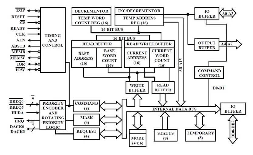
Block Diagram of 8237 Direct Memory Access (DMA) controller

Explain in detail the functioning of 8237 DMA controller

The 8237 DMA (Direct Memory Access) controller stands as a fascinating piece of electronic wizardry that revolutionized data transfer speeds in older computer systems. This ingenious device liberates the main CPU from the cumbersome task of shuttling data between memory and peripheral devices, offering a significant performance boost. Let’s embark on a journey to explore the inner workings of the 8237 DMA controller:

Block Diagram of 8237 DMA

This block diagram visually represents the major functional components of the 8237 DMA controller and their interactions.

What is DMA and why is it useful?

Imagine transferring a bucket full of books from one shelf to another. Conventionally, you’d pick up each book individually (CPU’s task), a slow and inefficient process. Alternatively, you could grab the entire bucket in one go (DMA’s task), minimizing individual movements and accelerating the process. In a computer system, the CPU frequently engages in data transfers between memory and peripherals, consuming valuable processing power. The 8237 DMA controller acts as the efficient “bucket carrier,” streamlining data transfer and enhancing overall system performance.

How does the 8237 DMA controller work?

Let’s break down the key steps involved:

  1. Channel Initialization:
    • The CPU configures the 8237 by programming its registers, setting parameters like source/destination memory addresses, transfer size, and transfer mode.
  2. DMA Request:
    • A peripheral device triggers a DMA transfer by sending a signal to the 8237, typically when data is ready to be sent or received.
  3. Channel Arbitration:
    • In case of simultaneous DMA requests from multiple devices, the 8237 prioritizes channels based on pre-programmed settings.
  4. Data Transfer:
    • Upon access approval, the 8237 seizes control of system buses, retrieves data from the source memory, increments the address, and writes the data to the destination memory until the transfer size is reached.
  5. DMA Acknowledgment:
    • Upon completion, the 8237 signals the CPU and the peripheral device, relinquishing control of the buses.

Benefits of using the 8237 DMA controller:

  • Increased System Performance:
  • By offloading data transfer tasks from the CPU, the 8237 significantly enhances overall system responsiveness.
  • Reduced CPU Load:
  • The CPU can focus on other tasks while the DMA controller efficiently handles data transfers, optimizing system efficiency.
  • Improved Data Transfer Rates:
  • Direct access to system buses enables faster data transfer compared to CPU-mediated methods.

In conclusion, the 8237 DMA controller remains a powerful relic that played a pivotal role in early computer systems, accelerating data transfer and improving overall performance. While its significance has waned in modern architectures with integrated DMA capabilities, understanding its workings provides valuable insights into the evolution of computer architecture and the perpetual quest for efficient data movement.

Architecture of 8259A: Diagram

Discuss the actions performed by 8086 when an interrupt is encountered by it? How 8259A can be used for multiple interrupts priority management? Draw and briefly explain the internal architecture of 8259A programmable interrupt controller.

Actions performed by 8086 when an interrupt is encountered

When the 8086 processor encounters an interrupt, it follows a series of steps to handle it. First, it completes the execution of the current instruction and then saves the flags and the contents of the registers onto the stack. After that, it fetches the address of the interrupt service routine (ISR) from the interrupt vector table (IVT). The processor then transfers control to the ISR to execute the specific task associated with the interrupt. Once the ISR is completed, the processor restores the saved register values and flags from the stack and resumes normal program execution.

Using 8259A for multiple interrupts priority management

The 8259A programmable interrupt controller is employed to manage multiple interrupts with different priorities. It allows for the prioritization of interrupts so that higher priority interrupts can be serviced before lower priority ones. The 8259A has multiple interrupt request lines (IRQs), and each IRQ can be assigned a specific priority level. By programming the 8259A, you can control which interrupts are enabled, their priority levels, and the interrupt service routine addresses associated with each interrupt.

Internal architecture of 8259A programmable interrupt controller

The 8259A consists of several key components, including:

  • Interrupt Request Register (IRR): This register stores the status of the interrupt lines, indicating which interrupts are currently pending.
  • In-Service Register (ISR): It keeps track of interrupts that are currently being serviced.
  • Interrupt Mask Register (IMR): This register allows you to enable or disable specific interrupt lines.
  • Control Word Register: Used for programming the 8259A. It includes information about the operating mode, whether it is edge or level triggered, and how the priorities are set.
  • Data Bus Buffer: Facilitates communication between the CPU and the 8259A.
  • Cascade Buffer: Used when multiple 8259A chips are connected to handle more than eight interrupts.

The 8259A can be cascaded to manage up to 64 interrupts by connecting multiple chips. Each 8259A can handle eight interrupts, and the master-slave configuration allows for the expansion of interrupt handling capabilities.

Interface a typical 12-bit DAC with 8255 and write a program to generate a square waveform of period 12 ms. The CPU runs at 3 MHz clock frequency.

To interface a typical 12-bit DAC (Digital-to-Analog Converter) with the 8255 programmable peripheral interface and Generating Square Wave with 12-Bit DAC and 8255, you need to follow several steps. The 8255 is a general-purpose I/O port chip, and you’ll use it to send data to the DAC to produce the desired waveform. Below is a step-by-step guide for Generating Square Wave with 12-Bit DAC and a simple program in assembly language for an Intel 8085 microprocessor, assuming you are using a CPU with a 3 MHz clock frequency.

Interfacing 12-bit Digital-to-Analog Converter (DAC) with 8255:

  1. Connect the DAC to Port A of 8255:
    • Connect the 8 data lines (D0-D7) of the DAC to Port A of the 8255.
    • Connect the DAC’s CS (Chip Select), WR (Write), and other control lines appropriately.
  2. Configure 8255:
    • Set the mode of Port A to output mode.
  3. Write Program for Generating Square Wave:
    • Write an assembly program to send the appropriate values to the DAC in a loop to generate a square wave.

Assembly Program:

ORG 0000H  ; Set the origin address
; Initialize 8255
MOV C, 82H  ; Control word for 8255 (Port A as output)
OUT 0F0H    ; Send control word to 8255
; Initialize variables
MOV B, 00H  ; Counter for square wave period
LOOP:
  ; Send high value to DAC (replace 3FFH with the desired 12-bit value)
  MOV A, 03FH  ; Data for DAC
  OUT 01H  ; Send data to Port A (connected to DAC)
  CALL DELAY  ; Delay function (half the square wave period)
  ; Send low value to DAC (replace 000H with the desired 12-bit value)
  MOV A, 000H  ; Data for DAC
  OUT 01H  ; Send data to Port A (connected to DAC)
  CALL DELAY  ; Delay function (half the square wave period)
  ; Increment counter and check for the desired period (adjust 30H for desired count)
  INX B
  CPI 30H  ; Check if the counter reached the desired count
  JZ RESET  ; If yes, reset the counter
  JMP LOOP  ; Repeat the loop
DELAY:
  ; Delay function (adjust the count for the desired delay)
  MOV B, 0FFH  ; Outer loop count
DELAY_LOOP:
  MOV C, 0FFH  ; Inner loop count
DELAY_INNER:
  NOP  ; No operation
  NOP  ; No operation
  NOP  ; No operation
  NOP  ; No operation
  NOP  ; No operation
  NOP  ; No operation
  NOP  ; No operation
  NOP  ; No operation
  NOP  ; No operation
  NOP  ; No operation
  DCR C  ; Decrement inner loop count
  JNZ DELAY_INNER  ; Repeat inner loop if not zero
  DCR B  ; Decrement outer loop count
  JNZ DELAY_LOOP  ; Repeat outer loop if not zero
  RET  ; Return from delay function
RESET:
  ; Reset counter
  MOV B, 00H
  JMP LOOP  ; Jump to the beginning of the loop

Explanation:

  1. Initialization:
    • The program starts by setting the 8255 control word, configuring Port A as an output port.
  2. Main Program Loop:
    • The main loop continuously sends data to the DAC to generate a high voltage level (full-scale output).
    • It then introduces a delay, followed by sending 0 to the DAC to generate a low voltage level.
    • Another delay follows. This process repeats, creating a square waveform.
  3. Delay Function:
    • The delay function is a simple nested loop that provides a delay. You may need to adjust the count for the delay based on the clock frequency of your CPU.
  4. Note:
    • This example assumes a 12-bit DAC. Adjust the data values and delay counts based on the specifications of your DAC and the desired waveform characteristics.

Instruction format and Generate HEX codes for | Mov Bx, [BX] [SI] | Mov Ax, Dx

Introduction

x86 assembly language, a low-level programming language that operates at the heart of your computer’s architecture. In this blog post, we’ll explore the instruction format and generate HEX codes for two common x86 instructions “Mov Bx, [BX] [SI] & Mov Ax, Dx”.

Instruction Format

Before we delve into the specific instructions, let’s understand the general format of x86 instructions. The x86 instruction format typically consists of:

  1. Operation Code (Opcode): This part specifies the operation to be performed.
  2. ModR/M: Stands for “Modifier Register/Memory.” It provides additional information about the operands.
  3. SIB (Scale Index Base): Used for more complex addressing modes involving scaling, indexing, and basing.
  4. Displacement: An offset or displacement value for memory addressing.
  5. Immediate Data: Immediate values used directly in the instruction.

Instruction 1: Mov Bx, [BX] [SI]

Let’s break down the instruction “Mov Bx, [BX] [SI]” into its components:

  • Opcode: The opcode for the MOV instruction is typically 8B (in hexadecimal).
  • ModR/M: In this case, the ModR/M byte is used to specify the addressing mode and the operands. The destination register is BX, and the source operand is located at the address formed by adding the contents of registers BX and SI.
  • SIB: Since there is an index (SI) involved, a SIB byte might be present, but in this case, it’s not necessary.
  • Displacement: Since there is no displacement, this part is 0.
  • Immediate Data: There is no immediate data for this instruction.

Now, let’s assemble these components:

  • Opcode: 8B
  • ModR/M: Assuming BX is the destination and [BX] [SI] is the source, the ModR/M byte would be 33 in hexadecimal (21 in decimal).
  • SIB: Not applicable (0)
  • Displacement: 0
  • Immediate Data: Not applicable

Putting it all together, the HEX code for “Mov Bx, [BX] [SI]” is 8B 33 00 00.

Instruction 2: Mov Ax, Dx

Now, let’s look at the “Mov Ax, Dx” instruction:

  • Opcode: Again, the MOV opcode is 8B.
  • ModR/M: Here, the destination register is AX, and the source register is DX.
  • SIB: Not applicable.
  • Displacement: 0
  • Immediate Data: Not applicable.

Assembling the components:

  • Opcode: 8B
  • ModR/M: Assuming AX is the destination and DX is the source, the ModR/M byte would be C2 in hexadecimal (194 in decimal).
  • SIB: Not applicable (0)
  • Displacement: 0
  • Immediate Data: Not applicable

The HEX code for “Mov Ax, Dx” is 8B C2 00 00.

Conclusion

Understanding x86 assembly language can be challenging, but breaking down instructions into their components helps demystify the process. By grasping the structure and meaning of each part, you’ll be well on your way to mastering low-level programming.

Sorting an Array in Descending Order using 8086 Assembly Language Programming (ALP)

8086 Assembly Language Programming (ALP) to solve a common problem: Sorting an Array using 8086 ALP of 10 bytes in descending order. Buckle up, and let’s explore the intricacies of this assembly language program.

Problem Statement

Imagine you have an array of ten bytes, and you want to arrange them in descending order. How do you do it using 8086 assembly language? Well, fear not! We’ve got the solution for you.

The Assembly Language Program

Let’s break down the assembly language program step by step.

section .data
    array   db  9, 3, 7, 1, 5, 2, 8, 4, 6, 0  ; The array to be sorted
    n       equ 10  ; Number of elements in the array
section .text
    global _start
_start:
    ; Display the original array
    mov cx, n        ; Initialize loop counter with the number of elements
    mov si, 0        ; Initialize source index to 0
display_array:
    mov dl, [array + si]  ; Load the element at array[si] into DL register
    add dl, '0'           ; Convert the numeric value to ASCII
    mov ah, 02h           ; Print character function
    int 21h               ; Invoke the interrupt to print the character
    ; Print a comma and space for clarity
    mov dl, ','
    int 21h
    inc si              ; Move to the next element in the array
    loop display_array ; Repeat until all elements are displayed
    ; Move to the next line
    mov ah, 02h   ; Print newline character function
    mov dl, 0Ah
    int 21h
    ; Sort the array in descending order
    mov cx, n  ; Initialize outer loop counter with the number of elements
outer_loop:
    mov si, 0  ; Initialize inner loop source index to 0
inner_loop:
    mov al, [array + si]      ; Load the current element into AL register
    cmp al, [array + si + 1]  ; Compare with the next element
    jge no_swap                ; Jump if greater than or equal, no swap needed
    ; Swap elements if needed
    mov ah, [array + si]       ; Load the next element into AH register
    mov [array + si], [array + si + 1]  ; Swap the elements
    mov [array + si + 1], ah
no_swap:
    inc si            ; Move to the next element in the array
    loop inner_loop   ; Repeat inner loop until all elements are compared
    dec cx            ; Decrement the outer loop counter
    jnz outer_loop    ; Repeat outer loop until all elements are sorted
    ; Display the sorted array
    mov cx, n
    mov si, 0
display_sorted_array:
    mov dl, [array + si]
    add dl, '0'   ; Convert to ASCII
    mov ah, 02h   ; Print character function
    int 21h
    ; Print a comma and space for clarity
    mov dl, ','
    int 21h
    inc si
    loop display_sorted_array
    ; Exit the program
    mov ah, 4Ch
    int 21h

Explanation:

  1. Initialization:
    • array: The array to be sorted.
    • n: Number of elements in the array.
  2. Display Original Array:
    • Loop through the array, converting each element to ASCII and printing it.
  3. Sorting in Descending Order:
    • Implementing a simple Bubble Sort algorithm:
      • Outer loop (outer_loop) iterates through each element.
      • Inner loop (inner_loop) compares adjacent elements and swaps them if needed.
  4. Display Sorted Array:
    • Similar to the display of the original array, this section prints the sorted elements.
  5. Exit the Program:
    • int 21h with function 4Ch is used to terminate the program.

Conclusion

And there you have it! A simple 8086 assembly language program to sort an array of bytes in descending order. Understanding the low-level operations involved in sorting algorithms can deepen your appreciation for the inner workings of computers.

Calculate Physical Addresses and Explain Addressing Modes | Microprocessor and Interfacing (MPI)

In this computational exercise, we calculate physical addresses and explain addressing modes of x86 assembly language programming, focusing on the calculation of physical addresses and the elucidation of various addressing modes. Given a scenario where the Data Segment (DS) is set to 5000H, we explore seven distinct instructions, ranging from immediate and register addressing to complex base register with displacement configurations. Each step involves deciphering the memory access pattern, shedding light on the nuanced addressing modes employed in the realm of assembly language programming.

Question: Compute the physical addresses that the following instructions will access. Assume that DS (Data Segment) is equal to 5000H, and the given memory operands are [CX] = 2000H, [SI] = 3000H, [BP] = 4000H, and [DI] = 1000H. Also, explain the addressing modes used by each instruction.

(i) MOV AX, [2000H]:

  • Addressing Mode: Immediate addressing.
  • Explanation: This instruction is directly loading the value at the memory address 2000H into the AX register. The physical address is 2000H.

(ii) MOV BX, AX:

  • Addressing Mode: Register addressing.
  • Explanation: This instruction copies the content of the AX register into the BX register. It does not involve memory access, so there is no physical address calculation.

(iii) MOV AX, [CX]:

  • Addressing Mode: Register indirect addressing.
  • Explanation: The content of the CX register is treated as a memory address, and the value at that address is loaded into the AX register. The physical address is 5000H (DS) + 2000H (content of CX) = 7000H.

(iv) MOV BX, [BP+DI]:

  • Addressing Mode: Base register addressing with displacement.
  • Explanation: The content of the BP register is used as a base address, and DI is added as a displacement. The physical address is 4000H (content of BP) + 1000H (content of DI) = 5000H.

(v) MOV BX, [BP+SI+6000H]:

  • Addressing Mode: Base register addressing with two displacements.
  • Explanation: The content of the BP register is used as a base address, SI is added as the first displacement, and 6000H is added as the second displacement. The physical address is 4000H (content of BP) + 3000H (content of SI) + 6000H = 13000H.

(vi) MOV AX, [BP]:

  • Addressing Mode: Base register addressing.
  • Explanation: The content of the BP register is used as a base address, and the value at that address is loaded into the AX register. The physical address is 4000H.

(vii) MOV AX, 3000H:

  • Addressing Mode: Immediate addressing.
  • Explanation: This instruction loads the immediate value 3000H directly into the AX register. It does not involve memory access, so there is no physical address calculation.

Simplify the Question and Answers for Better Understanding

Question: Imagine you have a computer system, and in this system, you are performing various operations with memory. In the context of your computer, you have a special area called the Data Segment (DS), which is set to 5000H. Additionally, you have specific values stored in different memory locations, like [CX] = 2000H, [SI] = 3000H, [BP] = 4000H, and [DI] = 1000H. Now, let’s explore some instructions:

(i) Move the contents of memory location 2000H into the AX register. What is the actual location in the computer’s memory that this instruction is talking about, and why?

  • Answer: The computer is going to the memory location 2000H to fetch a value and put it into the AX register. The location in the computer’s memory is 2000H.

(ii) Copy the contents of the AX register into the BX register. Where in the computer’s memory does this happen?

  • Answer: This operation doesn’t involve going to a specific memory location; it’s just copying data between registers. No memory address is needed.

(iii) Load the value from the memory location specified by the CX register into the AX register. What is the actual memory location in the computer, and how is it calculated?

  • Answer: The computer is looking at the memory location calculated by adding the contents of the CX register (2000H) to the Data Segment (DS) value (5000H). So, the location in the computer’s memory is 7000H.

(iv) Load the value from the memory location calculated by adding the contents of the BP and DI registers into the BX register. What is the actual memory location?

  • Answer: The computer calculates the memory location by adding the contents of the BP register (4000H) to the DI register (1000H). So, the location in the computer’s memory is 5000H.

(v) Load the value from the memory location calculated by adding the contents of the BP and SI registers and 6000H into the BX register. What is the actual memory location?

  • Answer: The computer calculates the memory location by adding the contents of the BP register (4000H), the SI register (3000H), and the immediate value 6000H. So, the location in the computer’s memory is 13000H.

(vi) Load the value from the memory location specified by the BP register into the AX register. What is the actual memory location in the computer?

  • Answer: The computer is looking at the memory location specified by the BP register (4000H). So, the location in the computer’s memory is 4000H.

(vii) Load the immediate value 3000H into the AX register. Does this involve going to a specific memory location?

  • Answer: No, this operation directly puts the value 3000H into the AX register without going to a specific memory location.

In summary, these instructions involve operations with memory, and the answers provide a simple explanation of the memory locations involved in each case.

Explain the following instructions with an example for each: (i) XLAT (ii) AND (iii) RCR (iv) DAA (v) AAS

(i) XLAT (Translate):

This instruction is used for table lookups. It takes the value in AL (the accumulator register) as an offset into a table and replaces the value in AL with the byte at the effective address.

Example:

MOV AL, 2      ; AL contains the offset
MOV BX, OFFSET Table ; BX points to the start of the table
XLAT           ; Replace AL with the byte at Table+2

(ii) AND (Logical AND):

This bitwise AND operation performs the logical AND between each pair of corresponding bits of the two operands. The result is stored in the destination operand.

Example:

MOV AX, 5      ; Binary: 0000 0101
AND AX, 3      ; Binary: 0000 0011
; After AND operation, AX will be: 0000 0001 (1 in decimal)

(iii) RCR (Rotate through Carry Right):

This instruction rotates the bits in the specified operand to the right through the carry flag. The carry flag is included in the rotation.

Example:

MOV AX, 8      ; Binary: 0000 1000
RCR AX, 1      ; Rotate AX right through carry by 1 bit
; After RCR operation, AX will be: 1000 0100 (carry will be set to 0)

(iv) DAA (Decimal Adjust Accumulator):

This instruction adjusts the contents of the AL register after an addition operation in packed decimal (BCD) arithmetic.

Example:

MOV AL, 90 ; AL contains unpacked BCD (9 in tens place, 0 in units place)
ADD AL, 25 ; Add 25 to AL (BCD addition)
DAA ; Adjust AL to correct BCD representation
; After DAA operation, AL will be: 15 (1 in tens place, 5 in units place)

(v) AAS (ASCII Adjust for Subtraction):

This instruction adjusts the result in the AL register after a subtraction operation in ASCII-coded decimal arithmetic.

Example:

MOV AL, '7'    ; AL contains ASCII representation of the digit 7
SUB AL, 3      ; Subtract 3 from AL (ASCII subtraction)
AAS            ; Adjust AL to correct ASCII representation
; After AAS operation, AL will be: '4' (ASCII representation of the digit 4)